
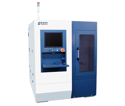
Silicon Carbide Wafer Laser Cutting Systerm
Uses ultra-short pulse laser to achieve high quality and high efficient cutting of silicon carbide wafer.
 Inquiry Phone:+86-400 8017 001
 E-mail:contact@delphilaser.com
■ Specifications:
◆ Processing object: silicon carbide wafers
◆ Laser type: Infrared picosecond pulsed laser
◆ Cooling method: air-cooled
◆ X-axis: stroke 450mm, resolution 0.1μm
◆ Y-axis: stroke 700mm, resolution 0.1μm
◆ Z-axis:stroke 20mm,resolution 0.1μm
◆ θ axis: travel 120°, resolution 0.001°
◆ Maximum cutting thickness: 500μm
◆ Maximum speed of cutting axis: 500mm/s
◆ Processing size: 6 inches(upgradeable to 8 inches)
■ Applications
Aerospace and Power Electronics Industries.
Specifically designed for cutting wafers with silicon carbide (SiC) substrates used in microwave devices and power devices.
■ Samples

For more information


