
Model:LUT-800; Laser mass transfer is used in the new display industry to transfer three-color chips to the substrate through direct transfer/secondary transfer.
To the product +
Model:LLO-8600; The system uses laser lift-off technology to peel off Micro LED wafers.
To the product +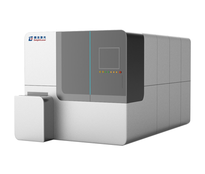
Model:DLDS-8680; The system is used for laser slicing processing of silicon carbide ingots/pieces. After the laser processing is completed, it is used with an auxiliary dicing device to complete wafer dicing after slicing. The material loss is small, while the processing efficiency is high. No consumables are required to operate the equipment, and the processing cost is low.
To the product +
Model:ALS03; The system is used for etching the internal series circuits of perovskite thin film solar cells. The system integrates a variety of laser sources and can complete P1/P2/P3 scribing and P4 edge cleaning in the perovskite cell production process.
To the product +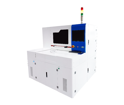
Model:CAT10; This system is designed for the automatic processing of insulation film removal in the battery cell rework process. It is equipped with a laser processing system and an automatic film removal system.
To the product +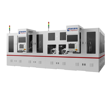
Model:LGC52; The system achieves high-speed and stable cutting of UTG through the customized development of a special optical shaping system and processing software.
To the product +
Model:LGC71; This system developed through special optical systems and processing software to achieve high-speed and stable cutting of curved glass.
To the product +
Model:DRP02/03/15; The equipment is designed for automated processing of large-format FPC (Flexible Printed Circuit) soft boards, cover films, COF (Chip on Film), CPI (Chip Package on Interposer), and adhesive products used in the automotive industry.
To the product +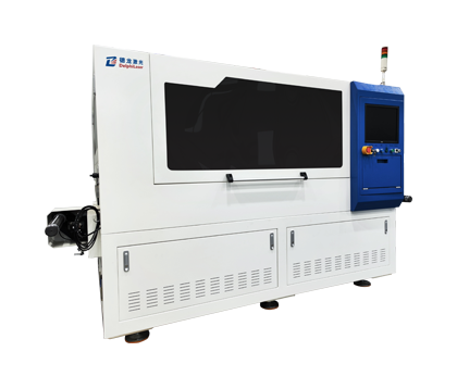

The system is mostly equipped with self-produced ultrafast lasers. Improve system performance, reduce cost and ensure timely delivery. We can develop laser with laser process.

More than ten years of accumulation of laser fine micro processing, providing laser solutions for various ultra-thin, ultra-hard, brittle, flexible and transparent materials.

Various transfer and robot handling technologies available,Many years of automation experience to provide customers with a stable automation operating environment.
Micro LED Wafer Laser Mass Transfer System
Micro LED Wafer Laser Lift Off System
Silicon Carbide Wafer Laser Processing System
Thin Film Solar Cell Laser Integrated Processing System
Battery Cell Film Laser Removal System
UTG Glass Laser Cutting System
HUD Curved Glass Laser Cutting System
Large-format Vehicle-mounted FPC/cover Film Roll-to-sheet Processing System
In the field of new electronics, it is mainly used in cutting, drilling, and etching flexible circuit boards (FPC), printed circuit boards (PCB), ceramics, electric vehicle glass, automotive head-up display glass, LCP/MPI antennas, PET thin films, etc. Especially along with the development of new energy vehicles, the demand for precision processing of related soft boards, vehicle glass, etc. has given rise to more applications of ultraviolet and ultrafast lasers. The company launches supporting laser processing solutions for applications in the fields of automotive electronics, 5G, and consumer electronics.
Electronics Industry
Some of our laser solutions for display applications include laser cutting, marking, drilling, repair, and the peeling of flexible materials, conductive films, glass, and other materials. These solutions are widely used in LCD, OLED, and Mini&Micro LED, covering all product sizes from 0.9 inches to 110 inches.
Display Industry
The variety of laser solutions for semiconductor applications includes stealth dicing of LEDs, wafers, Si wafers, and silicon carbide/gallium arsenide/gallium nitride; wafer/chip marking; TGV laser drilling; laser annealing; laser debonding; Micro LED laser lift-off (LLO); laser-based mass transfer; and laser repair. Materials that can be processed include compound semiconductor wafers made of diamond, sapphire, quartz, optical glass, silicon, silicon carbide, gallium arsenide, and gallium nitride among others.
Semiconductor Industry
In the field of new energy, we deploy new energy applications such as lithium-ion batteries and photovoltaics. Our solutions include: perovskite thin film solar cell production equipment; printing screen laser plate making equipment; intelligent equipment related to lithium-ion and hydrogen fuel power cells; power system energy storage, base station energy storage, and home energy storage battery-related intelligent equipment.
New Energy
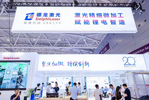
From May 15 to 17, 2025, the highly influential battery industry event - the 17th Shenzhen International Battery Fair (CIBF2025) was grandly held in Shenzhen. Delphi Laser showcased multiple advanced lithium battery manufacturing solutions including roll-to-roll laser baking equipment, roller press laser online cleaning systems, lithium battery echelon utilization, and 500W femtosecond lasers.Using precision laser micromachining technology to empower intelligent lithium battery manufacturing, Delphi Laser's booth attracted tremendous popularity and became the focal point of the exhibition! Focusing on details and continuous innovation. At this year's CIBF2025, Delphi Laser concentrated on technological innovation, bringing multiple industry-first innovative solutions that focused on the entire process upgrade in the lithium battery field, attracting extensive attention from numerous exhibition visitors and partners. During the exhibition, Delphi Laser also gave presentations on topics including laser drying, all-solid-state battery applications, ultrafast lasers, and battery pack laser disassembly processes, engaging in in-depth exchanges and discussions with many industry professionals on site to share the latest research and application achievements. Presentation scene Accepted live interview by Gaogong Cloud Exhibition Delphi Laser looks forward to meeting you next time! Please continue to follow Delphi Laser!
More +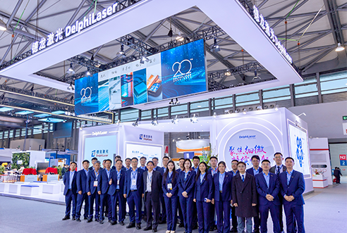
The 2025 LASER World of PHOTONICS CHINA successfully concluded. Delphi Laser, with innovative technologies and excellent products at its core, demonstrated cutting-edge laser solutions across multiple fields, receiving high recognition both within and outside the industry! Keynote Speeches During the exhibition, seven keynote speeches directly addressed industry pain points. Technical experts shared the latest R&D achievements and market prospects, creating an enthusiastic atmosphere on site! On-site Highlights Delphi Laser's booth was crowded with visitors. On-site audiences and partners experienced the charm of precision laser micro-processing up close, while jointly exploring its wide applications and future potential in the industry. On-site Activities The 2025 LASER World of PHOTONICS CHINA successfully concluded. Delphi Laser will continue to use "New Quality Productivity" as its engine, deepen laser applications and cutting-edge technologies, and drive innovative development in the industry!
More +
Recently, the China National Intellectual Property Administration (CNIPA) announced the eva1uation results of the 25th China Patent Awards. Suzhou Delphi Laser Co., Ltd. was honored with the "China Patent Excellence Award" for its patent titled "Device and Method for Asymmetric Beam Splitting Laser Processing of Transparent Materials", further demonstrating the company's strength in technological innovation. Since its establishment in 2005, Delphi Laser has consistently aligned with national R&D demands, placing high importance on intellectual property (IP) and actively advancing its IP-driven corporate strategy. The company has set up a dedicated IP management department, formulated strategic IP plans, and enhanced overall IP awareness. These efforts have earned it the titles of "National Intellectual Property Advantage Enterprise (2019)" and "National Intellectual Property Demonstration Enterprise (2022)". Moving forward, Delphi Laser will continue to uphold the principle of innovation-driven development, leverage its exemplary role, increase R&D investment, and actively explore new technologies and applications to enhance its core competitiveness. The company remains committed to achieving its goal of becoming a globally competitive IP powerhouse. About the China Patent Awards: Co-organized by the CNIPA and the World Intellectual Property Organization (WIPO), the China Patent Awards represent the only government-backed accolade in China that recognizes outstanding patented inventions. The awards aim to strengthen IP creation, protection, and utilization, promote high-quality economic development, and honor patentees and inventors (designers) who have made significant contributions to technological innovation and socio-economic progress.
More +


