

The system is mostly equipped with self-produced ultrafast lasers. Improve system performance, reduce cost and ensure timely delivery. We can develop laser with laser process.

More than ten years of accumulation of laser fine micro processing, providing laser solutions for various ultra-thin, ultra-hard, brittle, flexible and transparent materials.

Various transfer and robot handling technologies available,Many years of automation experience to provide customers with a stable automation operating environment.
In the field of new electronics, it is mainly used in cutting, drilling, and etching flexible circuit boards (FPC), printed circuit boards (PCB), ceramics, electric vehicle glass, automotive head-up display glass, LCP/MPI antennas, PET thin films, etc. Especially along with the development of new energy vehicles, the demand for precision processing of related soft boards, vehicle glass, etc. has given rise to more applications of ultraviolet and ultrafast lasers. The company launches supporting laser processing solutions for applications in the fields of automotive electronics, 5G, and consumer electronics.
Electronics Industry
Some of our laser solutions for display applications include laser cutting, marking, drilling, repair, and the peeling of flexible materials, conductive films, glass, and other materials. These solutions are widely used in LCD, OLED, and Mini&Micro LED, covering all product sizes from 0.9 inches to 110 inches.
Display Industry
The variety of laser solutions for semiconductor applications includes stealth dicing of LEDs, wafers, Si wafers, and silicon carbide/gallium arsenide/gallium nitride; wafer/chip marking; TGV laser drilling; laser annealing; laser debonding; Micro LED laser lift-off (LLO); laser-based mass transfer; and laser repair. Materials that can be processed include compound semiconductor wafers made of diamond, sapphire, quartz, optical glass, silicon, silicon carbide, gallium arsenide, and gallium nitride among others.
Semiconductor Industry
In the field of new energy, we deploy new energy applications such as lithium-ion batteries and photovoltaics. Our solutions include: perovskite thin film solar cell production equipment; printing screen laser plate making equipment; intelligent equipment related to lithium-ion and hydrogen fuel power cells; power system energy storage, base station energy storage, and home energy storage battery-related intelligent equipment.
New Energy

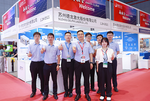
As a global trendsetter in the photovoltaic industry, the three-day 17th International Solar Photovoltaic and Smart Energy Conference & Exhibition (2024 SNEC) concluded successfully in Shanghai on June 15. Delphi Laser showcased perovskite thin-film solar cell laser applications, advanced crystalline silicon manufacturing solutions, and screen printing laser applications, attracting significant attention from exhibitors and industry clients worldwide. Perovskite GW Line Laser + Packaging Integrated Solution This equipment is used for etching the internal series circuit of perovskite thin-film solar cells. The equipment integrates multiple laser sources and can complete P1/P2/P3 scribing, P4 edge cleaning, P5 light-transmitting component processing, and P6 cutting and splitting in the perovskite cell production process. Roll-to-Roll Flexible Thin-Film Solar Cell Laser Scribing System This equipment is uses high-energy lasers for scribing on glass surfaces. Depending on the laser configuration, different processes can be performed. The equipment's components are efficiently integrated to achieve high-precision, high-speed scribing, and etching processes. BC Cell Laser De-coating Isolation Processing System This equipment is used for de-coating BC cells. It enhances the performance of the back passivation layer by reducing carrier recombination loss at the interface, thereby improving photoelectric conversion efficiency. TOPCon Laser Enhanced Sintering System This equipment is designed to improve contact resistance in crystalline silicon solar cells. It reduces metal-semiconductor recombination loss, improving the contact resistance between the electrode grid and the crystalline silicon cell, thereby enhancing the photovoltaic conversion efficiency of crystalline silicon cells. High-Precision Laser Screen Etching System This equipment is equipped with an ultrashort pulse UV laser, combined with high-performance peripheral components. It is primarily used for drilling and cutting PI and other materials. It can process photovoltaic and non-photovoltaic patterns on PI screens and is also capable of processing SE screens and knotless screens at the current stage. Delphi Laser looks forward to seeing you next time. Stay tuned to Delphi Laser!
More +
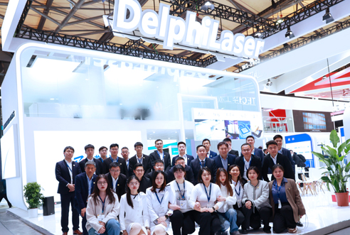
The three-day Laser World of Photonics China 2024 and SEMICON China 2024 have successfully concluded. Delphi Laser made a grand appearance with multi-field laser solutions, showcasing the company's achievements in technological development and product innovation, attracting numerous customers for communication and cooperation discussions! Let's take a look back at the highlights of this exhibition. ▼▼▼ At this year's photonics exhibition, Delphi Laser hosted six themed presentations focusing on laser precision micro-machining solutions, showcasing cutting-edge and innovative laser application cases, creating a lively atmosphere for on-site exchanges! Media Interviews Highlights from both exhibitions Delphi Laser looks forward to seeing you next time. Stay tuned to Delphi Laser!
More +
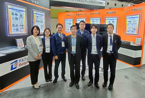
On May 8th, the Photonix 2024, an international photonics and laser exhibition in Japan, grandly opened at INTEX Osaka. Suzhou Delphi Laser Co., Ltd.'s wholly-owned subsidiary, Delphi Laser Japan Co., Ltd., showcased a variety of laser solutions once again at the exhibition. The event received widespread attention and high praise from both industry insiders and the general public! Delphi Laser looks forward to seeing you next time. Stay tuned to Delphi Laser!
More +


