
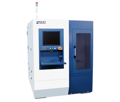
Wafer Laser Stress-Induced Dicing system
This system uses stress-induced cutting technology to process and cut Mini LED wafers.
 Inquiry Phone:+86-400 8017 001
 E-mail:contact@delphilaser.com
■ Specifications
◆ Laser type: DPSS picosecond laser
◆ Laser power: ≥1W
◆ Cooling method: Closed-loop water cooling
◆ X-axis: 360mm travel length, 0.1μm resolution
◆ Y-axis: 300mm travel length, 0.1μm resolution
◆ Z-axis: 15mm travel length, 1μm resolution
◆ θ-axis: ±60° travel angle, 0.0001° resolution
◆ Scribing speed ≤ 1000mm/s
◆ Throughput of 4-inche wafer:15pcs/h@10*30mil (4-inche wafer)
◆ Applicable wafer size: 2 or 4 inches (can be outfitted to 6-inch wafers)
◆ Optional dual spot processing capability
■ Advantages
◆ Fast cutting speeds, pause-less process
◆ High production capacity and yield rates, stable performance
◆ No consumables, Low operating costs
■ Applications
Straight Cutting of Sapphire Substrate Wafers for LED Lighting Industry
Straight Cutting of Sapphire Material for Other Industries
■ Samples

For more information


