

Model:LUT-800; Laser mass transfer is used in the new display industry to transfer three-color chips to the substrate through direct transfer/secondary transfer.
To the product +
Model:AWD20; This fully automated laser system is designed for Through-Glass Via (TGV) microhole processing on wafer-level glass substrates of various materials with thicknesses ranging from 0.1 to 1 mm. It supports the fabrication of various via structures, including blind holes and conical through-holes.
To the product +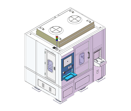
Model:ALS03; The system is used for etching the internal series circuits of perovskite thin film solar cells. The system integrates a variety of laser sources and can complete P1/P2/P3 scribing and P4 edge cleaning in the perovskite cell production process.
To the product +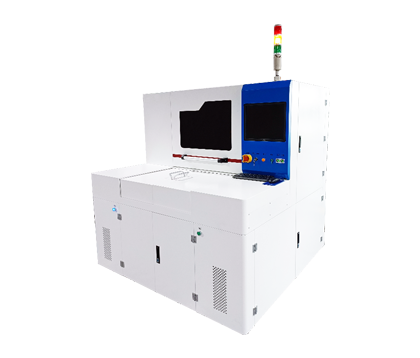
Model:APM12; The Fully Automatic Laser Marking Machine is designed for marking post-packaging products. It supports both slot magazine and stack magazine loading/unloading methods. Based on customer process requirements, the machine can be configured in 1-in-1-out or 2-in-2-out models.
To the product +
Model:PRC series; Special optical design, non-destructive roller surface, capable of matching maximum operating speed ≥120 meters per minute.
To the product +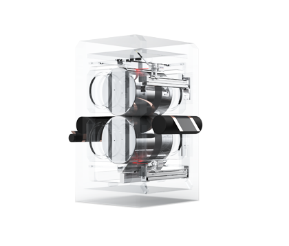
Model:RLH series; This system is primarily used for laser heating and dewatering of the positive and negative electrode sheets of lithium batteries.
To the product +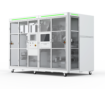
Model:LGC71; This system developed through special optical systems and processing software to achieve high-speed and stable cutting of curved glass.
To the product +
Model:FPS20/FPS24/FPS27; This equipment utilizes a high-energy customized laser to efficiently cut carbon fiber and other foldable display materials. The cut edges are smooth, burr-free, and free of burn marks, with fast processing speed. Equipped with an automatic vision positioning system and environmental safety features, the system ensures safe and high-speed automated cutting.
To the product +

The system is mostly equipped with self-produced ultrafast lasers. Improve system performance, reduce cost and ensure timely delivery. We can develop laser with laser process.

More than ten years of accumulation of laser fine micro processing, providing laser solutions for various ultra-thin, ultra-hard, brittle, flexible and transparent materials.

Various transfer and robot handling technologies available,Many years of automation experience to provide customers with a stable automation operating environment.
Micro LED Wafer Laser Mass Transfer System
Wafer-Level Laser Micro-Drilling System(TGV)
Thin Film Solar Cell Laser Integrated Processing System
Post-Molding Marking System(Rail-Type + Stack/Slot Loading/Unloading)
Laser Roller Cleaning System
Roll-to-Roll Laser Baking System
HUD Curved Glass Laser Cutting System
Carbon Fiber Cutting Application System
We offer laser applications for cutting, marking, drilling, etching, and welding on materials such as glass, ceramics, circuit boards (FPC/PCB), thin films, and metals—mainly for the automotive and consumer electronics sectors. For foldable devices, we provide comprehensive solutions covering cover glass, carbon fiber, metal hinges, OLED displays, circuit boards, and automation systems.
Electronics Industry
We primarily offer solutions for cutting and repair of TFT-LCD, AMOLED, and Mini LED displays, as well as peeling, transfer, and repair processes for Micro LED wafers.
Display Panel Industry
We mainly provide laser dicing for various wafer materials such as silicon, silicon carbide, gallium arsenide, lithium tantalate, lithium niobate, and glass. Key solutions include wafer laser grooving, silicon carbide ingot slicing, silicon carbide laser annealing, Through Glass Via (TGV), laser grooving (low-k), edge trimming, wafer marking, module drilling (TMV), laser debonding, and assisted welding for advanced packaging applications.
Semiconductor Industry
We have launched a range of innovative laser intelligent equipment for lithium battery manufacturing, including front-end process solutions and mid-to-back-end laser solutions. Our technology also supports solid-state battery production through roller cleaning and laser baking, and we provide precise disassembly solutions for lithium battery recycling and reuse.
Lithium Battery Industry
We supply complete production equipment for perovskite thin-film solar cells, including P0 laser marking, P1–P3 laser scribing, P4 edge deletion, material transfer and buffering systems, as well as downstream encapsulation and inspection equipment. We are also developing new products for crystalline silicon and BC cell photovoltaic technologies.
Photovoltaic Industry

With the explosive rise of large AI models, demand for optical transceivers has surged. As core data-transmission components in AI intelligent computing centers, optical transceivers evolve in lockstep with the advancement of computing power. As AI computing demand grows exponentially, high-speed optical modules—serving as the “critical conduit” for data transmission—are experiencing a rapid market boom. In the ongoing evolution of optical-module manufacturing toward higher density, higher precision, and lower cost, laser micromachining technologies are playing an irreplaceable role. Breakthroughs in Optical Communication Technologies Strengthen the Foundation for AI Computing Power and Optoelectronic Integration Recognizing the long-term growth potential of the optical-transceiver market, Delphi Laser entered the field in 2019 by developing laser-based manufacturing equipment. After years of technological accumulation, the company now provides customers in the optical-communication industry with a comprehensive portfolio of solutions—including laser cutting, drilling, depaneling, etching, solder-ball placement, welding, and bonding—along with automated dispensing & assembly, sorting, AOI inspection, and testing systems. These solutions play a critical role in the production of high-speed optical modules. Laser Micromachining Solutions In the manufacturing of 800G and 1.6T high-speed optical modules, Delphi Laser’s micromachining solutions enable high-precision fabrication of key components, ensuring high yield and high-density interconnects. This enhances the performance of optical-interconnect devices from the source and significantly improves optical-signal coupling efficiency and transmission quality. · Laser bonding systems target the wire-bonding process within optical modules, using high-precision, low-stress laser-interconnect methods to improve connection reliability and high-speed electrical-signal integrity. · Laser solder-ball welding and ball-mounting equipment enable electrical interconnection between chips (such as BGA or CSP) and PCBs. Through precise solder-ball placement and controlled reflow, the equipment forms reliable joints, achieving both mechanical attachment and electrical conduction between chip and PCB pads. · Laser depaneling systems deliver ultra-high positional accuracy, narrow cutting kerfs, and burr- and dust-free processing, minimizing mechanical stress and providing a strong foundation for automated downstream assembly. · Laser cutting systems leverage non-contact processing to avoid internal stress in components, resulting in smoother edges, higher precision, and better yield. They are suitable for materials such as glass, ceramics, and optical fiber. Automation Solutions · Multi-station automated assembly solutions enable highly efficient integration and flexible manufacturing across the optical-module production process. · Automated chip-sorting solutions ensure accuracy and consistency in chip screening and packaging. · Automated AOI inspection systems integrate optical detection with intelligent recognition to conduct comprehensive defect screening. · Automated testing equipment performs fast and thorough performance verification of finished modules. By integrating raw-material preparation, precision machining, intelligent assembly, chip sorting, defect inspection, and performance testing into a unified closed-loop system, Delphi Laser ensures that high-speed optical modules maintain exceptional quality and stability even under large-scale production. Looking ahead, as demand for high-speed optical modules continues to accelerate, Delphi Laser’s full-industry-chain solutions will remain a strong enabler of AI computing power development.
More +
Twenty years of perseverance through challenges, moving forward with determination; Twenty years of growth and achievement, illuminating a brilliant journey. In 2025, Delphi Laser reached the significant milestone of its 20th anniversary. From the first faint light in the laboratory to the brilliance of industrial application, Delphi Laser has remained true to its belief in “focusing on precision and driving continuous innovation.” With craftsmanship shaping quality and innovation lighting the way, we illuminate an intelligent future. Over the past two decades, we have lit dreams with light, traced the contours of our times with lasers, and written a magnificent chapter belonging to Dephi Laser through perseverance and dedication. On the occasion of this 20th anniversary, we celebrate with a grand series of Delphi Laser 20th Anniversary events, looking back on our journey, honoring those who strive, celebrating our achievements, and embarking on a new chapter ahead. 20th Anniversary Celebration · Marathon Carnival 20th Anniversary Celebration · Honor Gala Speeches by Mr. Masataka Uchida, President of UITech, and keynote address by Dr. ZHAO Yuxing, Founder of the Company The Power of Role Models Employee Stories New Journey Kick-off Ceremony Employees' Passionate Creations 20th Anniversary Celebration · Gala Dinner Employee-produced and performed programs Speeches by Mr. Chen Honglong, Guest, and Dr. ZHAO Yuxing, Company Founder Twenty years of accumulation reflect the strength of staying true to our original aspiration; twenty years of breakthroughs testify to the power of continuous innovation. From an early-stage pioneer at its founding to today’s industry-leading intelligent manufacturing innovator, Delphi Laser has always moved forward with the spirit of a true striver. Standing at a new starting point, the people of Delphi Laser will continue to uphold the mission of “Lasers are creating a micro world.” With technology as our wings and dreams as our steed, we ride forward with unstoppable momentum toward an even more brilliant future.
More +
On September 26, the “All-Solid-State Battery Intelligent Manufacturing Seminar,” organized by the China All-Solid-State Battery Industry-Academia-Research Collaborative Innovation Platform, was held in Beijing. The seminar focused on innovative breakthroughs in intelligent manufacturing for all-solid-state batteries. Delphi Laser’s Chairman Dr. Zhao Yuxing and the General Manager of the Lithium Battery Division Mr. Xu Haibin were invited to attend and deliver keynote presentations. Academician Ouyang Minggao, Professor at Tsinghua University and Chairman of the Collaborative Innovation Platform Dr. Zhao Yuxing, Chairman of Delphi Laser, delivering remarks Mr. Xu Haibin, General Manager of Delphi Laser’s Lithium Battery Division, presenting his keynote report Amid profound global transformations in the new-energy industry, all-solid-state batteries—renowned for their high safety, high energy density, and long cycle life—have become the strategic high ground in the global race for next-generation battery technologies. In the solid-state battery sector, Delphi Laser has leveraged its strong expertise and forward-looking deployment in ultrafast laser technologies to develop targeted solutions covering processes such as electrode insulation grooving and roller cleaning. At the same time, the company is accelerating the validation of new processes including dry-electrode laser preheating and ultrafast laser slitting to further empower the industry. Delphi Laser has been invited to become a member of the All-Solid-State Battery Intelligent Manufacturing Platform. Initiated by the All-Solid-State Battery Manufacturing Process and Equipment Alliance and jointly established by leading domestic lithium-battery equipment enterprises, the platform aims to build an open and shared experimental platform, collaboratively optimize solid-state battery manufacturing processes and equipment, and form a national-level “main force” for intelligent manufacturing. Looking ahead, Delphi Laser will continue to deepen the integration and innovation of ultrafast laser processing technologies with battery manufacturing, working hand in hand with industry, academia, and research partners to inject fresh momentum into the development of the industry.
More +


